 | |
| Part 5 - The IDE interface | |
|
I then decided to progress with the IDE interface. It happens while searching around I found Phil's website and his P.R.I.D.E ( wasn't called like that at time ) IDE interface. I loved it because it's simple to understand and is done without exotic components. Even if it did work as stated as soon as I finished to build it later on it turned out to be a source of a very weird bug that literally been an odissey for me to find out what it was. In reality I am still not 100% sure of what it was, probably caused by extra inductance of my wiring .. or something else, what was definitely looking to be was a kind of "double clocking" of the CS line when certain bytes patterns were present on the bus ( specifically a set of FFH followed by a set of 00H ). After literally trying "the impossible" I found out I was able to completely remove the bug by doing things like "output the NOT of what you just read on the bus", this bug also seemed to happen using full size IDE cables not shorter ones, it wasn't even happening with all the HDs I tried. In the end, by putting one more AND gate as buffer on the CS line made the problem completely disappeared. Maybe ground bounce, maybe that short delay added done something, mah .. |
1 2 3 4 5 6 7 |

|
|
| Phil's P.R.I.D.E interface also RAM,SIO,CTC | |
|
Despite all that Phil's interface gave me great satisfaction, after studing ATAPI Specifications and Phil's examples I was able to make my own assembler subroutines, at that point I was able to read/write sectors on disks and get device information. It was around this point I got this idea of "I want to use some standard", I did not like much the idea to begin to mess with an HD making it "unuseable for other purposes" so I took one step further, try to do something using a FAT32 file system. This is a story I'll explain better in my CP/M section, basically I wanted to use FAT32 files as "disk scratch area" to implement "virtual disks", I managed to do it and it does work. |
|
|
|
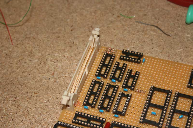
| IDE, components side and connector | |
|
In all and all I'd say I think this is one of the simplest IDE interfaces you can build that does the job and it's not terribly inefficient, if you really want do better than this then I'd say you HAVE to go for DMA or some more exotic solutions but as I said this is nice and uses standard TTL chips very easy to find and assemble. In the end also Phil "convinced" me to try the road of VHDL/CPLD/FPGA, I did not try FPGA yet but this is another story. |
|
|
|
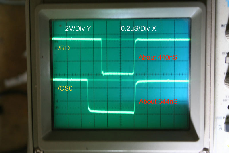
| The signals, nice and clean | |
|
Even before the AND gate you can see how signals were, however if it was a case of a ground bounce you can't see it "externally" by attaching an oscilloscope probe to anything it happens inside the chip. |
|
| Prev Back to Main Next | |
| page 5-7 | |